A lot of people are interested in how the computer starts up. This is where the magic begins and continues as long as the device is on. In this article, we will take an overview of the boot process, including its various stages, the key components involved, and the challenges faced during the process. While our primary focus will be on the x86 architecture (the most widely used), other architectures would have many similarities in their boot process. I hope this article would be a valuable resource for anyone looking to deepen their knowledge in this field. Here we go!
Contents:
- BOOT ROM
- Silicon Initialization
- Autonomous subsystems
- Hardware Power Sequences
BOOT ROM
An integrated circuit (chip) that is located onto the motherboard and stores the firmware code responsible for booting the computer is called BOOT ROM. This name is not standardized, so other developers often call it FLASH ROM, BIOS FLASH, BOOT FLASH, SPI FLASH, etc (such names are given to them because of the technology, interface and purpose names). It means the same thing, these terms are interchangeable. The firmware code in the BOOT ROM is executed first when the computer is powered on, and it performs basic tests, initializes the hardware, and then loads the OS-loader from a bootable device, such as a hard drive or a USB drive, into memory. This chip is made from non-volatile memory (NVM).
Non-Volatile Memory
Non-volatile memory is a type of computer memory that retains its contents even when the power is turned off. It makes this type of memory ideal for storing important data that need to be retained even when the computer is powered off. Furthermore, the discussion will be focused only on the memory that holds the firmware code. We will not talk about storage such as Hard Disk Drives (HDD), Solid State Drives (SSD), floppy disks, and so on.
Basically, we can categorize this type of memory into the following groups.
One Time Programmable
- Masked ROM: The contents are determined at the time of manufacture and cannot be changed after that.
- Programmable ROM (PROM): Unlike masked ROM, this type of memory can be programmed after manufacture. But still only once.
Field programmable
- Erasable Programmable ROM (EPROM): Сan be programmed multiple times, but its contents can be erased and reprogrammed using ultraviolet light.
- Electrically Erasable Programmable (EEPROM): Can be reprogrammed multiple times using electrical signals.
- NOR Flash memory: Architecturally arranged in blocks where data is erased at the block level and can be read or written at the byte level. NOR memory is directly accessible using a standard interface such as byte parallel, I2C or SPI.
In the industry, there is a convention to reserve the term EEPROM to byte-wise erasable memories compared to block-wise erasable flash memories.
With programmable memory come a one rule - erase before write. In such memory, writing new data is more complicated because the data is stored as charge on a floating gate (reason of it just lies in the physics of the memory cells). The amount of charge on the gate determines whether the cell stores "0" or "1". When you erase a flash memory chip, you set all the bits of data stored on it to a known (default) state, typically a logic "1". This allows you to start with a clean slate, so to speak, and program new data onto the chip without having any remnants of the old data still stored on it. When new data is written to the chip, the state of individual bits is changed from "1" to "0" to represent the new data.
If you simply write new data to the chip without first erasing it, the new data would be combined with the old data, resulting in unpredictable results. For example, consider a flash memory chip that has 8 bits of memory storing the value "0110 0010". If you write new data "1100 1001" to the chip without first erasing it, the resulting state of the chip would be "0100 0000", which may not be what you intended.
The main confusion is related to the word ROM which stands for Read Only Memory. The term "Read-Only Memory" has been historically used to refer to memory that is permanent and cannot be altered by the user. However, as technology has advanced, the definition of ROM has changed, and now it is often used to refer to memory that is pre-programmed at the factory and cannot be easily changed by the end user. But if the user has desired skills and specialized equipment (for example, programmer), the person can reprogram chip. The name ROM has remained, even though the definition has changed, as a historical reference to the original purpose of the memory.
By applying write protection, some types of reprogrammable ROMs may temporarily become read-only memory.
These are NOT ALL existing types of non-volatile memory, but most of the popular ones you might hear about just by chance. Nowadays, on most motherboards, these chips are made by using NOR Flash technology.
eXecute In Place (XIP)
Execute in Place (XIP) is a method that allows the processor to execute code directly from the flash memory without copying it into the volatile memory (such as RAM) first. This is achieved by mapping the flash memory into the processor's address space, so that code execution can be performed directly from the flash. So, the system is able to start executing code as soon as possible, without having to wait for the RAM to be initialized first.
Wait... the CPU can communicate with BOOT ROM via SPI/Parallel/etc protocol? Of course not, it is just fetching instructions from system memory, requests to this memory region are redirected to the Intel Direct Media Interface (DMI) or AMD Infinity Fabric (IF) / Unified Media Interface (UMI) (predecessor). It's link between the CPU and the chipset on the motherboard. At this point, decoding of the address is performed via decoders located in the chipset, and data from the chip is returned to the processor.
When the chip is made from NOR flash memory, which supports random access reads, but not random access writes came one problem. As far as writable memory isn't available, all computations have to be performed within the processor registers. At this point, the code can be written only in assembly language and it tend to set up environment for high-level language (typically, for C language). The reason for this is that memory initialization has become so complex, that it would be difficult to write purely in assembly. Since such languages require at least heap and stack, we need writable memory. Some processors have SRAM embedded on the chip itself, but a more modern approach is to use the onboard Cache memory As RAM (CAR).
Cache-As-Ram (CAR)
The CPU cache is a high-speed memory that stores a copy of frequently used data and instructions from main memory. A cache is located closer to the processor and organized into multiple levels (L1, L2, L3, ...), with each level being larger and slower than the previous one. If the data is in the cache, the CPU can retrieve the requested data from the cache (it's called cache hit). When the CPU cache is unable to find the required data, it results in a cache miss. This can occur either because the data was never stored in the cache, or because the data was previously stored but has been evicted from the cache. Anyway, the processor have to go all the way to main memory to access the data and copy it into the cache.
Cache eviction is the process of removing data from the cache to free up space for new data. The eviction of data can be initiated either by the caching system (typically, when a cache is full and new data needs to be stored, or when the data's time-to-live policy has expired) or by explicit request.
However, if we want to use the CPU Cache as RAM, we need to set up the cache to operate in Non-Eviction Mode, also called No-Fill Mode. This technique prevents eviction due to a cache miss. Instead, the cache is treated as a regular SRAM, and all accesses (read/write) will hit the cache and will not hit the main memory. The mode can be activated using vendor-specific CPU instructions.
Layout & Memory Mapping
In reality, the BOOT ROM contains several types of firmware. Once a bunch of firmware is stored in the BOOT ROM, it needs to be organized somehow to distinguish between them. Let's find out how it is done.
Non-Descriptor Mode
Originally, the chipset does a straight mapping of the entire BOOT ROM contents to memory (from 4GB to 4GB - 16MB). Typically, if the BOOT ROM is less than 16 MB, the contents are mapped repeatedly. The CPU and the firmware can read/write to the flash without any restrictions.
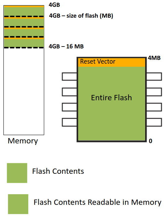
Non-Descriptor Mode is not supported anymore at new chipsets.
Intel Flash Descriptor / Descriptor mode
Eventually, in the ICH8, Intel introduces a special layout for BOOT ROM. The flash is divided to the following regions:
- Flash Descriptor (FD) - this data structure must be located in the beginning of the device with
0x10offset. It is made up of eleven sections as shown in the figure below: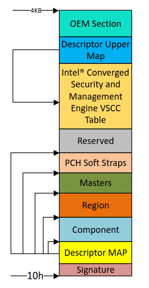
The Descriptor MAP has pointers to the other regions and the size of each as well.
The Component section has information about the flash(s) in the system (number of components, density of each, invalid instructions and so on).
The Masters section defines the read/write permissions for regions. As far as read/write permissions must be set to Read-Only, the information stored in this region can only be written during the manufacturing process.
For a better understanding of the details, I suggest you read this presentation by Open Security Training.
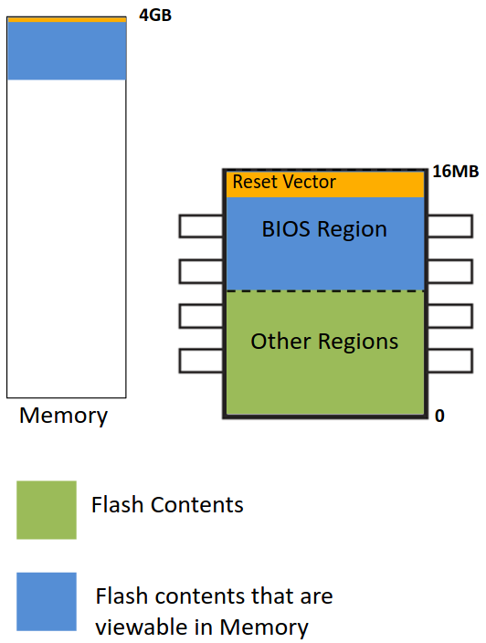
- BIOS - only this region is mapped into memory.
- Intel Converged Security and Management Engine (CSME / ME) - the firmware to support different Intel technologies and ME.
- Gigabit Ethernet (GbE) - can only be directly accessed by the Gigabit Ethernet controller.
- Platform data
- Embedded Controller (EC)
The Flash Descriptor and Intel ME are the only required regions.
Intel Firmware Interface Table (FIT)
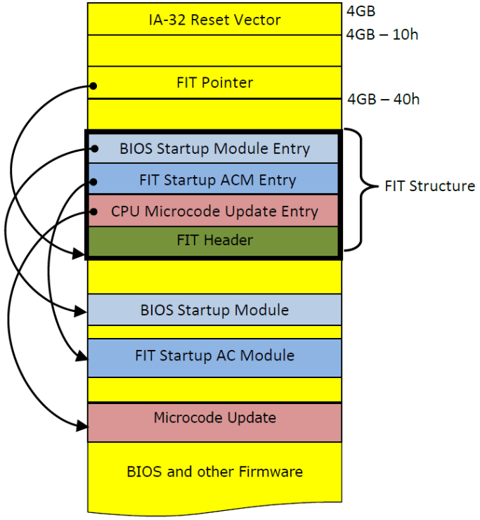
The FIT is a data structure inside the BIOS region and contains various entries that describe the platform configuration. Each entry in the table is 16 bytes in size. The first is called FIT header, the other are called FIT entry. It's located by a FIT pointer at physical address 0xFFFFFFC0 (4GB - 0x40).
These components must be processed before executing the first CPU instruction from the reset vector. Entries include CPU microcode updates, Startup ACM, Platform Boot/TPM/BIOS/TXT policies and other stuff. But at least the FIT should include FIT Header and Microcode Update entiries. So the common usage of FIT is to update the microcode before executing the reset vector. Here's what the memory map looks like:
As always, for more details use FIT specification 1.4.
AMD Embedded Firmware Structure
Unfortunately, there is much less information, I couldn't find any leaked AMD chipset documentation with details about their layout. So I can't tell you better than the coreboot documentation says. It is written based on AMD documentation which is only available under NDA.
Actually, it will be enough to know that the AMD analogue of Flash Descriptor is Embedded Firmware Structure and it contains pointers to the PSP Directory Table, BIOS Directory Table and other firmware.
Silicon Initialization
If you desired to take a look at how exactly modern memory and CPU are initialized, then I have to upset you. Intel and AMD are not in hurry to release the Silicon Initialization Code to the community. As far as such information is not publicly available, they offer binary distribution of necessary silicon initialization code. This is to be considered as a library for firmware developers and contains binary code to initialize the memory controller, the chipset, the CPU and other different parts of the system.
Intel Firmware Support Package (FSP)
That binary can be split up into 4 components:
- FSP-T: Setting up the early execution environment ("Temporary RAM") in which C code can be executed. In practice, this binary sets up CAR, but also does some early hardware initialization like setting up PCIe memory mapped configuration space.
- FSP-M: Initializing the permanent memory (such as DRAM).
- FSP-S: Completing the silicon initialization including CPU and IO controller initialization.
- FSP-O: Optional component that provide OEM devices initialization.
Repository of Intel FSP binaries posted by Intel you can find on their github. FSP Specification v2.1 can be obtained from the Intel website.
AMD Generic Encapsulated Software Architecture (AGESA)
AGESA for products earlier than Family 17h is known as v5 or Arch2008. At that time, AGESA was open sourced and the code was available in the coreboot repository (it was deprecated after release 4.18). The specification for Arch2008 can be found on the AMD website.
With the introduction of Family 17h (Zen microarchitecture) products, AMD has not been published AGESA source code, only prebuilt binary solutions. Such a successor is called AGESA v9 and supports for Family 17h and later.
openSIL
There is no detailed information available, only news.
Autonomous Subsystems
Integral part of the modern x86 boot process, without which the x86 cores would never be activated. Therefore it is impossible to completely disable them. This technologies are responsible for initialization hardware, verifying system integrity, power management, and launch of the CPU. The firmware for these subsystems are loaded and executed before the main processor starts executing its own firmware. A code on such systems runs independently from the CPU cores of the platform.
As long as many hardware companies have incorporated the principle of security through obscurity, neither the source code nor the documentation for these subsystems are available. Fortunately, we know how it affects the boot process - see Hardware Power Sequences.
We won't go into detail, because there are already extensive articles on the Internet from researchers all over the world. But I will just give you a brief description of what it is.
Intel Management Engine (ME)
Intel ME is a separate i486/80486 microprocessor integrated into the Intel chipset (PCH) since 2008 year. It has own RAM, built-in ROM, bus bridges to all of the buses inside the chipset (as result, it can access the network and even the main RAM on the CPU), and so on. Runs a custom OS based on MINIX.
AMD Platform Security Processor (PSP)
AMD PSP is an ARM core relying on Trustzone extension, which is inserted into the CPU die as a coprocessor. This chip is integrated on most AMD platforms since 2013 year. Runs a undocumented and proprietary OS.
Hardware Power Sequences
This process, also knows as Power On Sequence or Power Sequncing, provides a number of derived voltage levels and/or power supply rails in a particular order needed on the platform. In more simple term, it powers up a number of platform components in a specific order. The process varies depending on the system or platform design, but typically a standard PC includes the following steps:
- You press the power button. But wait... this button is on the computer case that is not a necessary part of a computer. Usually, the power button is a cable. We have a button on one side and a switch that we put on two metal prongs on the motherboard on the other side. When we press the button these prongs are connected so the electricity can go through them. Watch the video on how to turn on a computer without a power button if you're interested.
- The motherboard sends a signal to the power supply unit (PSU).
- Power supply receives the signal, provides the proper amount of electricity and sends a signal back to the motherboard.
- Once the motherboard receives the power good signal, it powers up platform components such as core, clocks, chipset, memory, different controllers, and so on.
- A variety of subsystems, including autonomous subsystems (discussed above), may starts prior to the main processor.
- AMD-based systems (for Family 17h and later)
- PSP executes on-chip BOOT ROM.
- PSP locates the Embedded Firmware Table in the off-chip BOOT ROM and executes PSP firmware.
- PSP parses the PSP Directory Table to find ABL stages and executes them.
- ABL stages initializes main memory, locates the BIOS image in the BOOT ROM and loads it into DRAM (decompresses if the image is compressed). This platform has no reason to use CAR because DRAM is already available and PSP loads the firmware image into it.
- Intel-based systems
- Chipset (ICH/PCH) finds the Intel Flash Descriptor in the BOOT ROM.
- Chipset copies CSME firmware into internal memory where Intel ME can access it and the last one starts executing it.
- Chipset maps the BIOS region to the memory.
- Microcode updates located in the Firmware Interface Table are loaded into the CPU. They have to be applied at each system boot.
- (optional) If Authenticated Code Modules (ACM) is found, then that entry is executed.
- All of this time, the CPU reset signal is asserted to prevent the CPU from starting before other parts of the system are ready. When the platform is ready, the CPU reset line is de-asserted. In a multi-processor or multi-core system one CPU is dynamically chosen to be the bootstrap processor (BSP) that runs all of the firmware initialization code. The remaining processors, called application processors (AP) at this point, remain halted until later on when they are explicitly activated by the firmware/kernel.
- After the CPU is first powered on, it operates in real mode. Most of the registers have well-defined values, including the Instruction Pointer (IP), the Code Segment (CS), and the Descriptor Cache, which is a copy of each segment descriptor within the processor to allow fast access to segment memory.
The Segment Descriptor is an entry in the Global Descriptor Table (GDT) and contains the base-address, segment limit and access information (this part is ignored because real mode doesn't have access control like the protected mode). Instead of accessing the GDT (which is located in the memory) for every memory access, the information is stored in a descriptor cache.
However, the GDT is not involved in real mode, so the processor generates entries internally. The CS selector register, used to access the segment descriptor, is loaded with0xF000. The CS base-address is initialized to0xFFFF_0000. IP is initialized to0xFFF0. Therefore, the processor begins fetching instructions from memory located at physical-address0xFFFF_FFF0(0xFFFF_0000+0x0000_FFF0). The first instruction executed at that address is called the reset vector.
NOTE: This trick gives you access to the high address space, however you cannot access the code below0xFFFF_0000address. The CS base-address remains at this initial value until the CS selector register is loaded by the firmware. It can be done by executing a far jump. At this point, the best decision is to switch to protected mode with 4 GB of addressability. If the firmware doesn't do it, then in order for real mode to work, the chipset must be able to alias a range of memory below 1 MB to an equivalent range just below 4 GB. Certain chipsets don't have this aliasing and may require a switch to another operating mode before the first long jump is performed.
- The address is in a section of non-volatile memory, so the CPU uses the Execute In Place (XIP) method. Although if it's an AMD-based system, you're probably reading from main memory.
- The CPU executes a firmware code.
I recommend you to watch this video about power-on sequence, which explains it using the ASUS P9X79 motherboard as an example. Despite the fact that it's in Russian language, you'll be able to understand everything if you turn on the auto-generated English subtitles
This article has provided a lot of theoretical information related to how booting works. However, to truly understand this process, we need to take a closer look at the source code and architecture of existing firmware. In the next article, we will delve deeper into BIOS, UEFI and coreboot to examine them in detail.
Resources
- Booting an Intel Architecture System, Part I: Early Initialization, web archive
- How Computers Boot Up
- ROM, EPROM, AND EEPROM TECHNOLOGY
- Differences Between EEPROM and NOR Flash
- A gentle introduction to Cache-as-Ram on X86
- Pictures about non-descriptor and descriptor mode are derived from Xeno Kovah's 'Architecture 4001: x86-64 Intel Firmware Attack & Defense' class, which was derived from John Butterworth & Xeno Kovah's 'Advanced Intel x86: BIOS and SMM' class